Reconfigurable MEMS-Based High-Impedance Surfaces for Millimetre and Submillimetre Wave Phase Shifters
D. Chicherin (1) , S. Dudorov (1) , D. Lioubtchenko (1) , V. Ovchinnikov (2) , A.V. Räisänen (1)
(1) Department of Radio Science and Engineering / SMARAD, Aalto University School of Electrical Engineering, Finland, (2) Microelectronics Centre, Aalto University, Finland
Introduction
Many millimetre wave applications such as point-to-point radio link or automotive radars require controllability or scanning of the beam direction. This can be done by phase array antenna, where the phase of each element is controlled by a phase shifter. We propose to use reconfigurable MEMS-based high-impedance surface in order to create phase shifters by introducing it into the waveguides.
Reconfigurable MEMS-based high-impedance surface

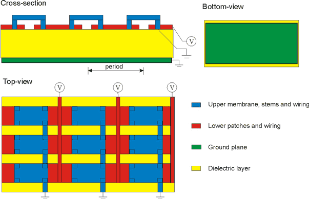
Fig. 1: Reconfigurable MEMS-based high-impedance surface
- Period << ? => we can use effective surface impedance model
- effective resonant circuit parameters: L and C
- At the resonant frequency ? = 1/( LC ) 0.5
- Surface impedance tends to imaginary infinity
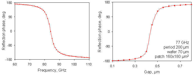
- Phase of the electric field reflection coefficient of an incident plane wave changes from ±180° to zero

Fig. 2: Frequency dependence of the high-impedance surface reflection phase, simulated (lhs)
and dependence of the high-impedance surface reflection phase on the gap between the upper and lower patches, simulated (rhs)
Phase shifter with MEMS-based high-impedance surface

Fig.3: Phase shifter based on a rectangular metal waveguide with MEMS-based high-impedance surface placed along side walls
- Effective propagation constant is changed in the high-impedance section
- Phase shift occurs when
- High-impedance is tuned from high impedance state to low impedance state, or
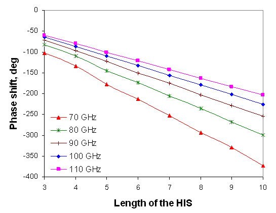
- Length of the high impedance section is tuned
- Analogue type phase shifter

Fig.4: Dependence of the phase shift on the length of the high-impedance surface introduced along the narrow walls of the rectangular metal waveguide, simulated
Fixed prototype of the MEMS-based high-impedance surface
We manufactured a prototype of the MEMS-based HIS consisted of a dielectric layer placed on a ground plane, and two arrays of metal patches, see Fig. 5. The gap between the upper and lower array of patches was fixed and filled with SiO 2 . The period of the structure was 120 µm, the thickness of the dielectric layer was 20 µm, and the gap between upper and lower patches was 0.24 µm. The patches' material was Al.

Fig. 5: Cross section (lhs) and optical image (rhs) of the manufactured fixed MEMS-based high-impedance surface prototype
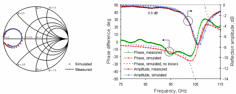
The samples were placed as a backshort of a WR-10 waveguide. The phase and the amplitude of the reflected wave were measured with a HP 8510 Vector Network Analyser at frequencies 75 – 110 GHz. Near the resonance frequency the phase changes by 50 degrees, and the losses of the prototype at frequencies when it performs as an electric wall (i.e. when the equivalent surface impedance is low), are below 0.5 dB The results of measurement and simulation presented in Fig. 6 are in a good agreement .

Fig. 6: Smith chart and frequency dependence of the measured and simulated results of the S 11 parameter of the fixed MEMS-based high-impedance surface prototype

